Description
ZEISS GeminiSEM is a family of field emission scanning electron microscopes (FE-SEM) designed for the highest demands in sub-nanometer imaging, analytics, and flexible sample handling. The system combines ultra-high resolution, efficient signal detection, and broad configuration capabilities for complex scientific and applied tasks.
GeminiSEM is intended for users who require not only high-quality electron imaging but also comprehensive sample characterization — from surface topography to material contrast, elemental composition, crystallography, and nanoscale structural features. Thanks to ZEISS Gemini electron optics, in-column Inlens detection, advanced analytical configuration, and support for complex, sensitive, and non-conductive samples, the system delivers consistently high performance across a wide range of applications.
Key Features
- Field emission FE-SEM platform for sub-nanometer imaging and advanced analysis
- High resolution at low accelerating voltages, including below 1 kV
- Flexible combination of topographical, compositional, elemental, and crystallographic information
- Efficient work with sensitive, non-conductive, magnetic, and complex multi-material samples
- Support for automated workflows, correlative microscopy, 3D STEM tomography, and in situ experiments
Technologies
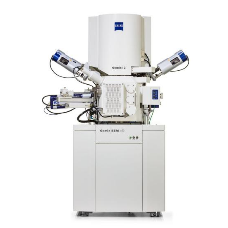
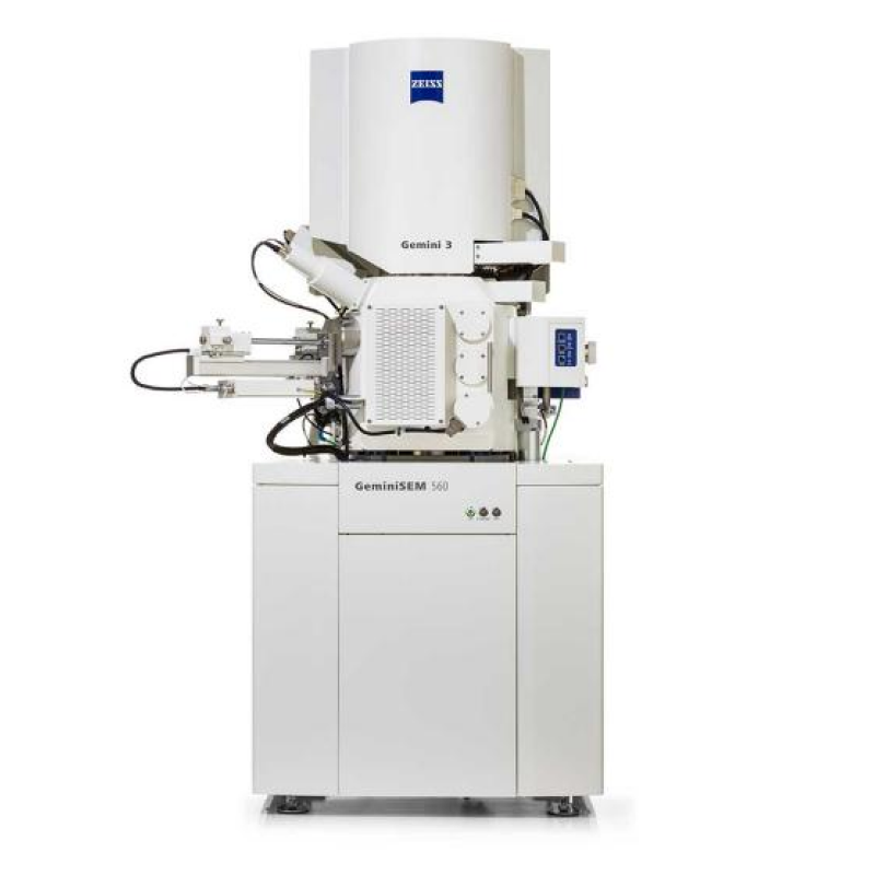
- ZEISS Gemini electron optics: a family of Gemini 1, Gemini 2, and Gemini 3 electron-optical columns for different imaging and analytical scenarios
- Inlens detection: highly efficient in-column detection of secondary and backscattered electrons for surface-sensitive imaging and material contrast
- NanoVP / Variable Pressure: modes for investigating non-conductive and sensitive samples without loss of image quality
- Smart Autopilot and Nano-twin lens: advanced electron optics for maximum resolution and simplified operation, especially in GeminiSEM 560
- EDS / EBSD / WDS / aSTEM / Atlas 5 / ZEN core: an extended ecosystem for analytics, correlative microscopy, automation, 3D visualization, and large-scale data workflows
Applications
- Materials science, nanomaterials, and functional surfaces
- Energy materials, batteries, catalysts, polymers, and composites
- Industrial microscopy, failure analysis, fractography, and metallography
- Electronics, semiconductors, device analysis, and subsurface structures
- Life sciences research, cell and tissue ultrastructure, serial sections, and block-face imaging
Advantages
- Premium FE-SEM class: a solution for applications requiring maximum detail, contrast, and analytical flexibility
- Sub-nanometer resolution: ultra-high image quality even at low accelerating voltages
- Deep analytical capability: combines SEM imaging with elemental, crystallographic, and structural analysis
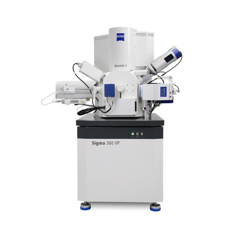
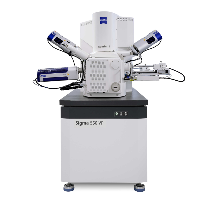
- Family flexibility: GeminiSEM 360, 460, and 560 configurations allow adaptation to universal, analytical, or highly surface-sensitive tasks
- Scalability and expandability: support for additional detectors, automation, multimodal, and 3D workflows