Description
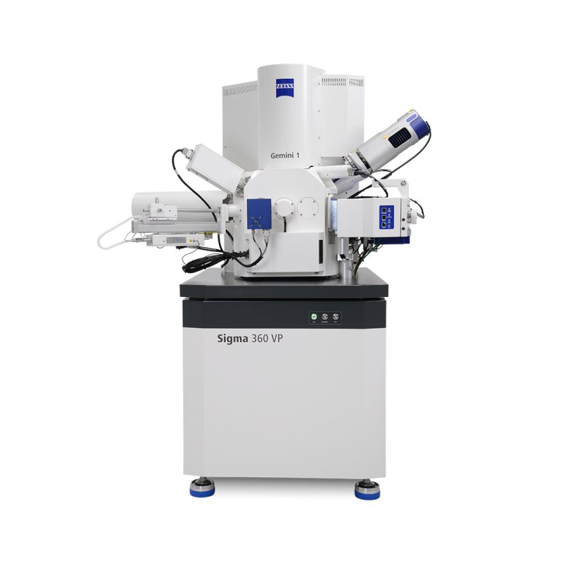
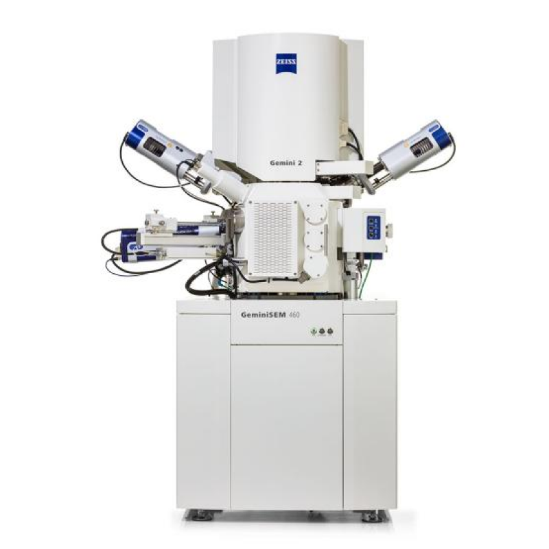
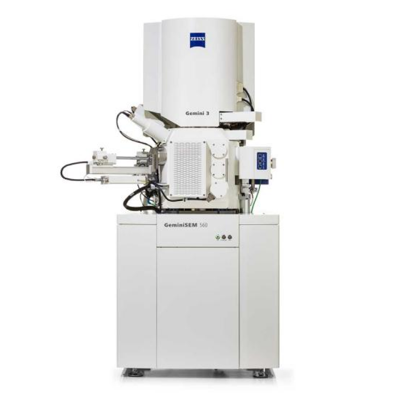
ZEISS Sigma is a family of field emission scanning electron microscopes (FE-SEM) designed for high-quality imaging and advanced analysis. The system combines high resolution, efficient low-voltage operation, and flexible analytical capabilities for research and industrial applications.
Sigma is intended for users who require not only SEM imaging but also precise sample characterization at the micro- and nanoscale. With ZEISS Gemini 1 electron optics, a wide range of detectors, support for Variable Pressure and NanoVP lite modes, the system delivers reliable results even when working with delicate, non-conductive, or complex samples.
Key Features
- Field emission FE-SEM platform for high-resolution imaging and analysis
- High resolution at low accelerating voltages, including 1 kV and below
- Advanced capabilities for elemental, crystallographic, and morphological analysis
- Efficient imaging of non-conductive samples without mandatory coating
- Support for automated workflows, AI-based analysis, and multimodal microscopy
Technologies
- ZEISS Gemini 1 optics: high-resolution electron optics with small probe size and efficient Inlens detection
- Low-kV imaging: enhanced detail and contrast at low accelerating voltages for surface-sensitive imaging
- NanoVP lite: advanced variable pressure mode for imaging and analysis of non-conductive samples with improved signal-to-noise ratio
- Flexible Detection: wide range of detectors for topographical, compositional, and structural information
- ZEN core / RISE / SmartPI / Mineralogic: software and analytical ecosystem for correlative microscopy, Raman imaging, particle analysis, and automated mineralogy
Applications
- Materials science and nanomaterials
- Energy materials, batteries, catalysts, polymers
- Life sciences research
- Geology, mineralogy, and natural resource analysis
- Industrial microscopy, failure analysis, quality control, and particle analysis
Advantages
- High-end FE-SEM class: transition from routine imaging to nanoscale analytics
- Excellent low-kV performance: more surface information with reduced sample damage
- Analytical flexibility: integration of EDS, EBSD, WDS, Raman, and other techniques
- Handling complex samples: efficient imaging of non-conductive and sensitive materials
- Scalability: Sigma 360 and Sigma 560 configurations allow adaptation to specific laboratory needs