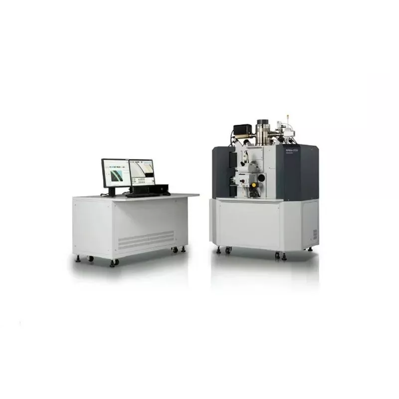
Description
Electron Probe Microanalyzers
The new generation of devices for high-precision X-ray spectral analysis of nano- and micro-objects allows obtaining surface images in scanning electron microscopy (SEM) mode — using secondary or backscattered electrons. It enables both qualitative and quantitative elemental analysis, mapping of element distribution by area and concentration, and identification of elements in trace amounts, including information on chemical state and bonding type.
Features
- The instrument features an increased X-ray detection angle (52.5°), improving analytical performance by providing better spatial resolution and higher sensitivity due to reduced X-ray absorption.
- Optimized for the analysis of uneven or rough samples, minimizing signal loss when examining depressions or textured surfaces.
- The microanalyzer offers exceptional stability and reproducibility, serving as a reference standard for microanalysis. Sensitivity for certain elements reaches tens of ppm.
- A built-in optical microscope with approximately 540× magnification, coaxial and confocal with the electron probe, allows simultaneous observation of SEM and optical images with true color rendering.
- The use of high-efficiency Johansson crystal analyzers ensures perfect convergence without aberration.
- The device can accommodate up to five 4-inch wavelength-dispersive spectrometers covering the full spectral range.