Description
ZEISS Crossbeam is a family of FIB-SEM (Focused Ion Beam–Scanning Electron Microscope) systems that combine high-resolution electron imaging with precision ion beam processing. The platform is designed for applications where it is necessary not only to observe material structures but also to precisely modify them at the micro- and nanoscale.
Crossbeam provides a complete workflow—from locating the region of interest to precise sample preparation and subsequent analysis. The combination of ZEISS Gemini electron optics, the Ion-sculptor ion column, and automated workflows enables complex analytical and technological tasks to be performed with high reproducibility, even for delicate and multi-component specimens.
Crossbeam systems cover a broad range of applications, from versatile research tasks to high-precision TEM lamella preparation and automated industrial workflows, including serial processes with minimal operator influence.
Key Features
- Combination of SEM imaging and ion beam processing within a single system
- Real-time monitoring of ion milling processes using electron imaging
- Precision sample preparation, including fabrication of nanometer-thin TEM lamellae
- Minimal structural damage through low-energy ion processing
- Automated workflows and parameter-driven operations for stable and reproducible results
Technologies
- ZEISS Gemini electron optics: high-resolution electron optics for detailed imaging of surfaces and internal structures, including low-voltage operation
- Ion-sculptor FIB: ion column for precise ion beam processing and polishing with minimal specimen damage
- Live SEM monitoring: real-time imaging during ion processing for workflow control and accurate targeting of regions of interest
- Automation and recipe-based workflows: automated workflows with batch processing capabilities and result standardization
- Low-kV imaging: gentle surface imaging with reduced impact on the specimen
Applications
- Microelectronics and semiconductors — failure analysis, investigation of internal layers, and TEM sample preparation
- Materials science — analysis of microstructures, defects, phase boundaries, and complex multiphase materials
- Sample preparation for transmission electron microscopy (TEM)
- 3D reconstruction of material structures and biological specimens
- Nanofabrication and nanoscale material modification
- Industrial research and standardized sample preparation in production environments
Advantages
- Complete control: simultaneous imaging and ion beam processing of the specimen
- High precision: nanometer-scale sample preparation and accurate endpoint detection
- Minimal damage: preservation of the true material structure, even for sensitive samples
- Reproducibility: consistent results regardless of operator experience through automation
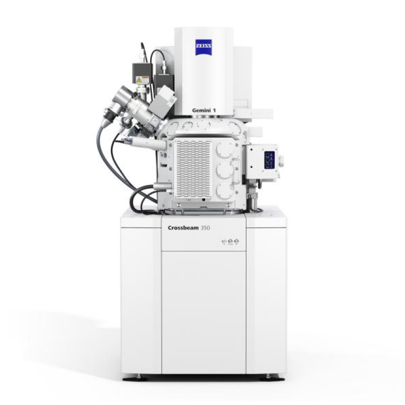
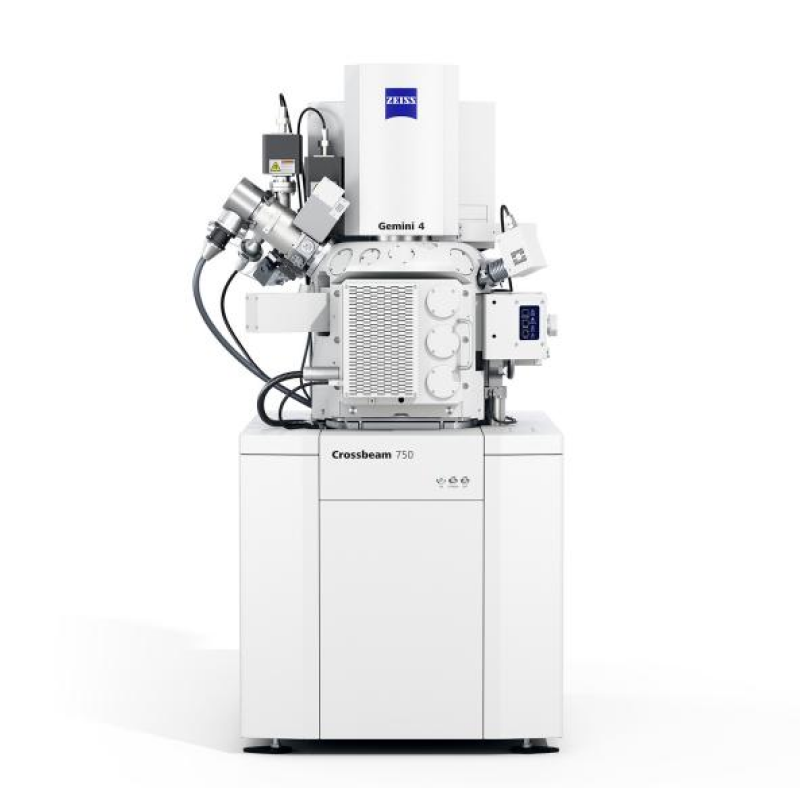
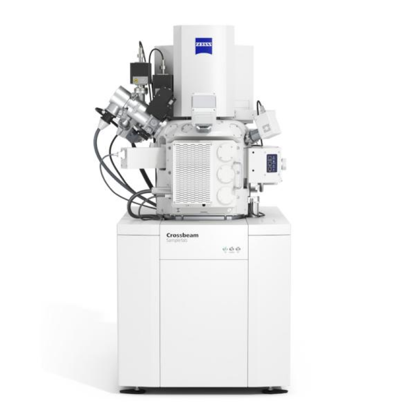
- Flexibility: Crossbeam 350, 550, 750, and Samplefab configurations can be tailored to applications ranging from general-purpose research to high-precision and fully automated workflows